Device tour
Seven parts on the board do all the work. Hover or tap a marker to highlight what it points at.
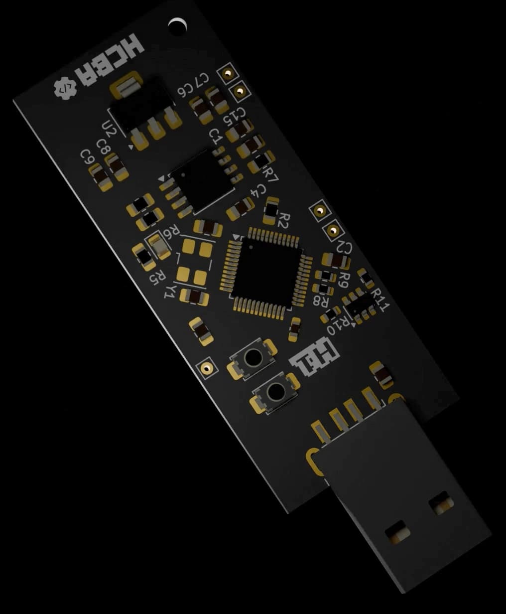
- USB-A connectorPlugs directly into a host port. Carries both power and data — it is the only physical connection H1 needs.
- STM32 microcontrollerRuns the H1 firmware: USB HID and CDC enumeration, and script execution.
- Onboard NOR flashStores your compiled scripts. Persists across power cycles, so running a new script never means reprogramming the device.
- Upload button
- Reset button
- Status LEDA single onboard LED, fully controllable from your script with LED_ON and LED_OFF.
- Crystal oscillatorMarked Y1. Provides a stable clock reference for the STM32.
The render above is the current bare development PCB (prototype revision). The production version will ship inside an enclosed, thumb-drive-style housing.
Where to read more
- The two buttons, and what each one does at boot and during execution: Buttons.
- The status LED and how a script drives it: LEDs.
- How much script the onboard flash holds: Flash variants.
- What the USB-A connector carries in each mode: USB-A port.
Last updated on